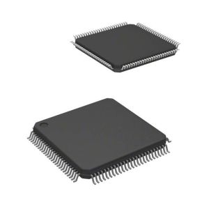
LCMXO2-2000HC-4TG144C Integrated Circuit Chip FPGA 111 I/O 144TQFP
Chips from factories. All are new and original. Pls inform us the part number and qty when to inquiry.
Specifications of LCMXO2-256HC-4TG100I
| TYPE | DESCRIPTION |
| Category | Integrated Circuits (ICs) |
| | Embedded |
| | FPGAs (Field Programmable Gate Array) |
| Mfr | Lattice Semiconductor Corporation |
| Series | MachXO2 |
| Packaging | Tray |
| Number of LABs/CLBs | 32 |
| Number of Logic Elements/Cells | 256 |
| Number of I/O | 55 |
| Voltage - Supply | 2.375V ~ 3.465V |
| Mounting Type | Surface Mount |
| Operating Temperature | -40°C ~ 100°C (TJ) |
| Package / Case | 100-LQFP |
| Supplier Device Package | 100-TQFP (14x14) |
| Base Product Number | LCMXO2-256 |
Features of LCMXO2-256HC-4TG100I
• High Performance, Flexible I/O Buffer
• Programmable sysIO™ buffer supports wide range of interfaces:
– LVCMOS 3.3/2.5/1.8/1.5/1.2
– LVTTL
– PCI
– LVDS, Bus-LVDS, MLVDS, RSDS, LVPECL
– SSTL 25/18
– HSTL 18
– Schmitt trigger inputs, up to 0.5 V hysteresis
• I/Os support hot socketing
• On-chip differential termination
• Programmable pull-up or pull-down mode
• Flexible On-Chip Clocking
• Eight primary clocks
• Up to two edge clocks for high-speed I/O interfaces (top and bottom sides only)
• Up to two analog PLLs per device with fractional-n frequency synthesis
– Wide input frequency range (7 MHz to 400 MHz)
• Non-volatile, Infinitely Reconfigurable
• Instant-on – powers up in microseconds
• Single-chip, secure solution
• Programmable through JTAG, SPI or I2C
• Supports background programming of non-vola�tile memory
• Optional dual boot with external SPI memory
• TransFR™ Reconfiguration
• In-field logic update while system operates
• Enhanced System Level Support
• On-chip hardened functions: SPI, I2C, timer/counter
• On-chip oscillator with 5.5% accuracy
• Unique TraceID for system tracking
• One Time Programmable (OTP) mode
• Single power supply with extended operating range
• IEEE Standard 1149.1 boundary scan
• IEEE 1532 compliant in-system programming
• Broad Range of Package Options
• TQFP, WLCSP, ucBGA, csBGA, caBGA, ftBGA, fpBGA, QFN package options
• Small footprint package options
– As small as 2.5 mm x 2.5 mm
• Density migration supported
• Advanced halogen-free packaging
Descriptions of LCMXO2-256HC-4TG100I
MachXO2 devices provide commonly used hardened functions such as SPI controller, I2
C controller and timer/
counter. MachXO2-640/U and higher density devices also provide User Flash Memory (UFM). These hardened
functions and the UFM interface to the core logic and routing through a WISHBONE interface. The UFM can also
be accessed through the SPI, I2
C and JTAG ports.
Environmental & Export Classifications of LCMXO2-256HC-4TG100I
| ATTRIBUTE | DESCRIPTION |
| RoHS Status | ROHS3 Compliant |
| Moisture Sensitivity Level (MSL) | 3 (168 Hours) |
| REACH Status | REACH Unaffected |
| ECCN | EAR99 |
| HTSUS | 8542.39.0001 |

Product Tags:

|
|
LCMXO2-256HC-4TG100I MachXO2 Field Programmable Gate Array (FPGA) IC 55 256 100-LQFP Images
|